- 您现在的位置:买卖IC网 > Sheet目录3890 > PIC16C774T-E/L (Microchip Technology)IC MCU OTP 4KX14 A/D PWM 44PLCC
PCA9534_3
NXP B.V. 2006. All rights reserved.
Product data sheet
Rev. 03 — 6 November 2006
10 of 25
NXP Semiconductors
PCA9534
8-bit I2C-bus and SMBus low power I/O port with interrupt
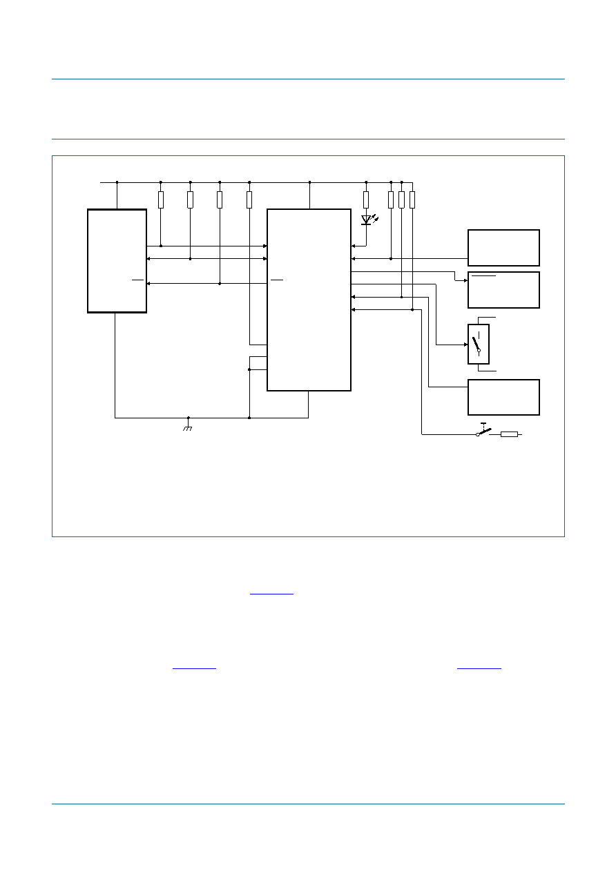
7.
Application design-in information
7.1 Minimizing IDD when the I/O us used to control LEDs
When the I/Os are used to control LEDs, they are normally connected to VDD through a
resistor as shown in Figure 12. Since the LED acts as a diode, when the LED is off the
I/O VI is about 1.2 V less than VDD. The supply current, IDD, increases as VI becomes
lower than VDD.
Designs needing to minimize current consumption, such as battery power applications,
should consider maintaining the IOn pins greater than or equal to VDD when the LED is
less than the LED supply voltage by at least 1.2 V. Both of these methods maintain the
I/O VI at or above VDD and prevents additional supply current consumption when the LED
is off.
Device address congured as 0100 100X for this example.
IO0, IO1, IO2 congured as outputs.
IO3, IO4, IO5 congured as inputs.
IO6, IO7 are not used and must be congured as outputs.
Fig 12. Typical application
PCA9534
IO0
IO1
SCL
SDA
VDD
002aac476
SCL
SDA
IO2
IO3
VDD
VSS
MASTER
CONTROLLER
VSS
VDD (5 V)
2 k
SUBSYSTEM 1
(e.g., temp. sensor)
INT
SUBSYSTEM 2
(e.g., counter)
RESET
controlled switch
(e.g., CBT device)
A
B
enable
INT
5 V
INT
10 k
10 k
SUBSYSTEM 3
(e.g., alarm system)
ALARM
IO4
IO5
VDD
A2
A1
A0
IO6
IO7
100 k
(
× 3)
10 k
10 k
发布紧急采购,3分钟左右您将得到回复。
相关PDF资料
PIC16F74T-E/L
IC MCU FLASH 4KX14 A/D 44PLCC
PIC16C765T-I/L
IC MCU OTP 8KX14 USB 44PLCC
PIC18C442T-E/L
IC MCU OTP 8KX16 A/D 44PLCC
PIC16C621A-40/SS
IC MCU OTP 1KX14 COMP 20SSOP
PIC16C622A-40/SS
IC MCU OTP 2KX14 COMP 20SSOP
PIC16CE623-30/SO
IC MCU OTP 512X14 EE COMP 18SOIC
PIC16CE624-30/SO
IC MCU OTP 1KX14 EE COMP 18SOIC
PIC16CE624-30/SS
IC MCU OTP 1KX14 EE COMP 20SSOP
相关代理商/技术参数
PIC16C774T-E/PQ
功能描述:8位微控制器 -MCU 7KB 256 RAM 33 I/O RoHS:否 制造商:Silicon Labs 核心:8051 处理器系列:C8051F39x 数据总线宽度:8 bit 最大时钟频率:50 MHz 程序存储器大小:16 KB 数据 RAM 大小:1 KB 片上 ADC:Yes 工作电源电压:1.8 V to 3.6 V 工作温度范围:- 40 C to + 105 C 封装 / 箱体:QFN-20 安装风格:SMD/SMT
PIC16C774T-E/PT
功能描述:8位微控制器 -MCU 7KB 256 RAM 33 I/O RoHS:否 制造商:Silicon Labs 核心:8051 处理器系列:C8051F39x 数据总线宽度:8 bit 最大时钟频率:50 MHz 程序存储器大小:16 KB 数据 RAM 大小:1 KB 片上 ADC:Yes 工作电源电压:1.8 V to 3.6 V 工作温度范围:- 40 C to + 105 C 封装 / 箱体:QFN-20 安装风格:SMD/SMT
PIC16C774T-I/L
功能描述:8位微控制器 -MCU 7KB 256 RAM 33 I/O RoHS:否 制造商:Silicon Labs 核心:8051 处理器系列:C8051F39x 数据总线宽度:8 bit 最大时钟频率:50 MHz 程序存储器大小:16 KB 数据 RAM 大小:1 KB 片上 ADC:Yes 工作电源电压:1.8 V to 3.6 V 工作温度范围:- 40 C to + 105 C 封装 / 箱体:QFN-20 安装风格:SMD/SMT
PIC16C774T-I/PQ
功能描述:8位微控制器 -MCU 7KB 256 RAM 33 I/O RoHS:否 制造商:Silicon Labs 核心:8051 处理器系列:C8051F39x 数据总线宽度:8 bit 最大时钟频率:50 MHz 程序存储器大小:16 KB 数据 RAM 大小:1 KB 片上 ADC:Yes 工作电源电压:1.8 V to 3.6 V 工作温度范围:- 40 C to + 105 C 封装 / 箱体:QFN-20 安装风格:SMD/SMT
PIC16C774T-I/PT
功能描述:8位微控制器 -MCU 7KB 256 RAM 33 I/O RoHS:否 制造商:Silicon Labs 核心:8051 处理器系列:C8051F39x 数据总线宽度:8 bit 最大时钟频率:50 MHz 程序存储器大小:16 KB 数据 RAM 大小:1 KB 片上 ADC:Yes 工作电源电压:1.8 V to 3.6 V 工作温度范围:- 40 C to + 105 C 封装 / 箱体:QFN-20 安装风格:SMD/SMT
PIC16C77T-04/L
功能描述:8位微控制器 -MCU 14KB 368 RAM 33 I/O RoHS:否 制造商:Silicon Labs 核心:8051 处理器系列:C8051F39x 数据总线宽度:8 bit 最大时钟频率:50 MHz 程序存储器大小:16 KB 数据 RAM 大小:1 KB 片上 ADC:Yes 工作电源电压:1.8 V to 3.6 V 工作温度范围:- 40 C to + 105 C 封装 / 箱体:QFN-20 安装风格:SMD/SMT
PIC16C77T-04/PQ
功能描述:8位微控制器 -MCU 14KB 368 RAM 33 I/O RoHS:否 制造商:Silicon Labs 核心:8051 处理器系列:C8051F39x 数据总线宽度:8 bit 最大时钟频率:50 MHz 程序存储器大小:16 KB 数据 RAM 大小:1 KB 片上 ADC:Yes 工作电源电压:1.8 V to 3.6 V 工作温度范围:- 40 C to + 105 C 封装 / 箱体:QFN-20 安装风格:SMD/SMT
PIC16C77T-04/PT
功能描述:8位微控制器 -MCU 14KB 368 RAM 33 I/O RoHS:否 制造商:Silicon Labs 核心:8051 处理器系列:C8051F39x 数据总线宽度:8 bit 最大时钟频率:50 MHz 程序存储器大小:16 KB 数据 RAM 大小:1 KB 片上 ADC:Yes 工作电源电压:1.8 V to 3.6 V 工作温度范围:- 40 C to + 105 C 封装 / 箱体:QFN-20 安装风格:SMD/SMT